



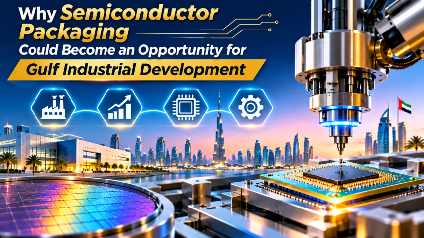
Why GCC Countries Are Exploring Semiconductor Industry Opportunities
Across the Gulf Cooperation Council, governments are investing in advanced manufacturing, digital infrastructure, artificial intelligence, and industrial diversification. While semiconductor manufacturing has traditionally been associated with established technology centres in Asia, the United States, and Europe, changes within the global industry are creating new discussions about where different stages of chip production could take place.
- 1. Why Semiconductor Packaging in the Gulf Is Becoming a Strategic Opportunity
- 2. How Advanced Packaging and Chiplets Are Changing the Semiconductor Industry
- 3. What Saudi Arabia’s Semiconductor Initiatives Reveal About Industrial Potential
- 4. How the UAE Could Connect Semiconductor Packaging With Advanced Manufacturing
- 5. How Packaging Could Support Gulf Manufacturing, Skills and Supply Chains
- 6. The Financial, Technical and Environmental Challenges of Semiconductor Packaging
- 7. The Future of Semiconductor Packaging in GCC Industrial Diversification
- Conclusion
One area attracting increasing attention is semiconductor packaging.
For many years, chip packaging was viewed primarily as the final stage of semiconductor manufacturing. Today, advanced packaging technologies are becoming important to how processors deliver higher performance, manage energy consumption, and combine different computing functions.
This development could create opportunities for countries seeking to enter selected parts of the semiconductor value chain without immediately constructing the most advanced wafer fabrication plants.
Semiconductor packaging in the Gulf could potentially support industrial development through specialised assembly operations, testing facilities, electronics integration, materials production, engineering services, and technical research.
Saudi Arabia has launched a National Semiconductor Hub intended to develop domestic chip design capabilities. The UAE is also promoting advanced manufacturing, with Abu Dhabi identifying semiconductors as a strategic growth sector.
These initiatives could provide foundations for related industrial activities.
However, establishing a competitive packaging industry is not straightforward. Semiconductor assembly and testing require specialised equipment, clean manufacturing environments, reliable utilities, skilled workers, international customers, and strict quality standards.
The technology also differs considerably between conventional chip packaging and the most advanced systems used in high-performance AI processors.
For Gulf countries, the opportunity may therefore involve identifying commercially realistic activities rather than attempting to replicate every part of the global semiconductor industry at once.
Understanding the role of packaging reveals how selected investments, research partnerships, and manufacturing capabilities could contribute to a broader regional electronics ecosystem.
1. Why Semiconductor Packaging in the Gulf Is Becoming a Strategic Opportunity
Semiconductors are essential components in modern electronics. They support mobile phones, vehicles, industrial equipment, telecommunications networks, medical devices, renewable energy systems, and data centres.
However, the semiconductor industry involves several distinct stages.
Designers develop electronic circuits, fabrication facilities produce semiconductor structures on wafers, and assembly and testing specialists turn those devices into usable components.
Understanding Semiconductor Packaging
Semiconductor packaging is the process of preparing a manufactured chip for integration into an electronic system.
A package may provide electrical connections, physical protection, thermal management, and mechanical support.
Packaging also helps connect the semiconductor device with a circuit board or another component.
In modern applications, packaging can influence the performance and reliability of the complete system.
Why Packaging Is No Longer Just Protective
Traditional packaging focuses on protecting and connecting individual semiconductor devices.
Advanced packaging can combine several semiconductor dies within one integrated assembly.
These dies may perform different functions, including processing, memory, communications, or specialised acceleration.
Such approaches can help manufacturers design complex systems without necessarily producing every function on one large silicon die.
The Global Semiconductor Value Chain
| Stage | Main Activity | Typical Requirements |
|---|---|---|
| Chip Design | Develop electronic circuits | Engineering and design software |
| Wafer Fabrication | Manufacture semiconductor devices | Highly specialised factories |
| Wafer Testing | Identify working devices | Precision testing equipment |
| Assembly and Packaging | Protect and connect chips | Materials, equipment and process controls |
| Final Testing | Verify electrical performance | Test systems and quality procedures |
| Electronics Integration | Incorporate chips into products | Electronics manufacturing capabilities |
Why Entry Points Matter
The most advanced wafer fabrication facilities involve enormous capital requirements and sophisticated supply chains.
Packaging also requires substantial investment, especially for advanced technologies.
However, selected packaging, testing, and electronics assembly activities may offer different investment scales and technical pathways.
The commercial opportunity depends on which activities a country can perform competitively.
2. How Advanced Packaging and Chiplets Are Changing the Semiconductor Industry
Semiconductor designers face growing pressure to improve computing performance while controlling power consumption, heat, and manufacturing costs.
Advanced packaging is becoming one way to address these challenges.
Understanding Chiplets
A chiplet is a relatively small semiconductor die designed to operate as part of a larger system.
Rather than producing every component on one large chip, designers may combine multiple chiplets.
Some may perform different functions or be manufactured using different fabrication processes.
This approach is known as heterogeneous integration when different technologies are combined into one system.
However, chiplet-based products require carefully engineered connections, compatible interfaces, and suitable testing.
Two-and-a-Half-Dimensional Packaging
2.5D packaging commonly places multiple semiconductor dies close together using an interposer or another advanced connection structure.
This can support high-bandwidth communication between components.
It is relevant to certain high-performance computing and AI systems.
However, the manufacturing processes are substantially more demanding than those used for many conventional packages.
Three-Dimensional Integration
3D integration can involve stacking semiconductor dies vertically.
This may reduce the physical distance between components and increase integration density.
However, thermal management, alignment, testing, and manufacturing yield become especially important.
A technically impressive design is not necessarily economical to manufacture at commercial volumes.
Advanced Packaging Technologies Compared
| Technology | Main Application | Technical Challenge |
|---|---|---|
| Conventional Packaging | Individual chip protection and connection | Cost and reliability |
| Wafer-Level Packaging | Packaging processes applied at wafer scale | Precision and yield |
| Fan-Out Packaging | High-density electrical connections | Process control |
| 2.5D Integration | Closely connected multiple dies | Interposers and interconnects |
| 3D Integration | Vertically stacked components | Heat and alignment |
| Chiplet Packaging | Integration of separately manufactured dies | Interfaces and system testing |
Why AI Demand Matters
AI processors increasingly require high-speed connections between processing and memory components.
Advanced packaging can help enable these architectures.
Reuters reported on November 6, 2026, that increased AI-related demand was intensifying competition for advanced packaging capacity.
Industry researchers cited in the report forecast significant capital expenditure on the technology.
However, rising international investment does not automatically establish a profitable market for a new Gulf-based facility.
Any regional project would need customers, proven technical capabilities, and a commercially viable operating model.
3. What Saudi Arabia’s Semiconductor Initiatives Reveal About Industrial Potential
Saudi Arabia provides an important example of a GCC country developing a semiconductor-related research and investment ecosystem.
Its activities currently place substantial emphasis on design, skills, research, and collaboration.
The National Semiconductor Hub
Saudi Arabia established the National Semiconductor Hub in June 2024.
The initiative is coordinated through the Research, Development and Innovation Authority and related institutional partnerships.
Its objective is to develop an integrated semiconductor ecosystem, bringing together universities, research organisations, technology companies, investors, and government entities.
The hub has identified the development of specialised chip design companies as a central priority.
Skills and Investment Targets
At the 2024 launch, Saudi authorities identified objectives including attracting or developing 50 semiconductor design companies and training and employing 5,000 engineers by 2030.
These are strategic targets rather than confirmed completed outcomes.
They demonstrate the scale of the Kingdom’s ambitions but should not be treated as evidence of a fully established domestic semiconductor manufacturing industry.
The Role of Research Institutions
The King Abdulaziz City for Science and Technology and King Abdullah University of Science and Technology have supported semiconductor research and collaboration.
The Future of Semiconductors Forum has brought together researchers and industry participants to discuss chip design, manufacturing, packaging, and emerging computing technologies.
Research activity can help build technical knowledge.
However, commercial manufacturing requires additional investment and industrial capabilities.
An Important 2026 Development
In April 2026, Semafor reported that Saudi industrial investment company Alat had dropped certain plans to invest in semiconductor production after difficulties securing major manufacturing partnerships.
This report is relevant because it demonstrates that ambitious semiconductor investment proposals can face commercial and strategic obstacles.
It should not be interpreted as meaning all Saudi semiconductor research and design initiatives have ended.
The National Semiconductor Hub continues to describe its mission around ecosystem development.
Possible Packaging Opportunities in Saudi Arabia
A developing chip design ecosystem could eventually generate demand for prototype assembly, packaging design, reliability testing, and specialised engineering services.
However, such services would require actual customers and appropriate technical partnerships.
Saudi Semiconductor Development Areas
| Initiative | Main Focus | Relationship to Packaging |
|---|---|---|
| National Semiconductor Hub | Design ecosystem and investment | Potential future customer and research links |
| KACST Research | Semiconductor technologies | Technical expertise |
| KAUST Collaboration | Research and specialist skills | Packaging-related research potential |
| Electronics Manufacturing Initiatives | Advanced industrial production | Possible adjacent supply chains |
| International Partnerships | Technology and investment cooperation | Access to specialist capabilities |
The strongest initial opportunity may involve connecting design expertise with testing and specialised electronics services before attempting the most technically demanding packaging operations.
4. How the UAE Could Connect Semiconductor Packaging With Advanced Manufacturing
The UAE has developed an industrial strategy focused on expanding advanced manufacturing and strengthening technology-intensive economic activity.
Its semiconductor opportunity needs to be understood within this wider environment.
Operation 300bn
The UAE’s Operation 300bn strategy aims to increase the industrial sector’s contribution to GDP from AED 133 billion to AED 300 billion by 2031.
The strategy supports advanced manufacturing, technology adoption, and industrial competitiveness.
However, the AED 300 billion figure is a national industrial target, not a semiconductor packaging investment commitment.
Abu Dhabi’s Semiconductor Strategy
Abu Dhabi’s Department of Economic Development identifies semiconductors as a strategic growth sector.
The emirate has experience with international semiconductor investment through Mubadala.
Its wider economic environment also includes research institutions, technology companies, logistics infrastructure, and industrial development zones.
However, international investments in semiconductor companies should not be confused with the physical location of semiconductor packaging factories.
The Importance of Industrial Infrastructure
Packaging and testing facilities require dependable electricity, cooling, clean production environments, reliable materials, and efficient logistics.
Industrial zones may provide some of this supporting infrastructure.
However, an ordinary manufacturing building is not automatically suitable for semiconductor assembly.
Facilities must be designed around specific process and quality requirements.
Potential Links With Regional Electronics Demand
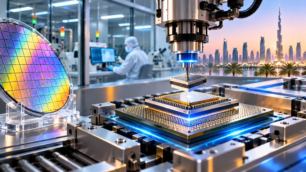
The UAE is expanding sectors involving data centres, telecommunications, energy technologies, and advanced electronic systems.
These industries rely on semiconductor components.
Local demand for electronic products could help inform investment decisions, particularly for specialised modules and system integration.
However, purchasing imported chips for data centres does not automatically create local demand for packaging those chips.
The commercial relationship must be established.
Possible UAE Development Pathways
| Activity | Potential Connection |
|---|---|
| Semiconductor Packaging Design | Engineering and research capabilities |
| Electronics Assembly | Existing manufacturing infrastructure |
| Component Testing | Reliability and product verification |
| Power Electronics Modules | Energy and industrial applications |
| Materials and Substrates | Specialised industrial supply chains |
| Advanced Packaging Research | University and technology partnerships |
Why Commercial Partnerships Matter
A Gulf-based packaging facility would likely need relationships with chip designers, wafer manufacturers, equipment suppliers, and downstream electronics companies.
Without such partnerships, access to industrial premises and capital would be insufficient.
5. How Packaging Could Support Gulf Manufacturing, Skills and Supply Chains
Semiconductor packaging could create opportunities extending beyond the companies operating assembly facilities.
The sector requires a network of supporting businesses and technical professionals.
However, these opportunities should be evaluated according to actual demand rather than assumed economic multipliers.
Developing Engineering Skills
Semiconductor packaging involves expertise in electrical engineering, materials science, mechanical engineering, chemical processes, automation, and quality control.
Specialists may work on package design, thermal performance, testing, process optimisation, and failure analysis.
GCC universities could contribute through relevant courses and applied research.
However, developing a skilled workforce requires practical industrial experience alongside classroom training.
The Role of Small and Medium-Sized Enterprises
SMEs may provide selected supporting services to semiconductor packaging operations.
These could include precision engineering, equipment maintenance, logistics, software integration, industrial automation, or technical services.
Some activities may require specialist certifications or extensive training.
Companies should avoid assuming that every existing manufacturing supplier can immediately serve semiconductor customers.
Materials and Components
Packaging can require substrates, bonding materials, encapsulation compounds, electrical connections, and thermal management components.
These supply chains are technically demanding.
Developing domestic production of selected materials could create industrial opportunities, provided businesses can meet global quality and cost requirements.
Opportunities Around Testing
Semiconductor testing is an important part of verifying that devices perform according to specification.
Testing facilities may examine electrical performance, operating characteristics, or reliability under selected conditions.
However, semiconductor qualification requirements differ by device and application.
For example, components intended for demanding industrial environments may require testing that is unnecessary for some consumer products.
Potential Industrial Benefits
| Development Area | Possible Contribution |
|---|---|
| Engineering Employment | Specialist technical careers |
| Materials Manufacturing | Higher-value industrial products |
| Equipment Maintenance | Advanced service capabilities |
| Testing Laboratories | Quality and reliability services |
| Industrial Automation | Precision manufacturing expertise |
| University Partnerships | Applied research and training |
| Electronics Integration | Greater downstream manufacturing capability |
Why Supplier Development Is Important
Packaging facilities cannot operate efficiently without dependable suppliers.
Gulf industrial programmes focused on local content and manufacturing capability could potentially support suitable businesses.
However, local sourcing requirements should not compromise semiconductor quality, reliability, or safety.
A competitive industrial ecosystem must meet the standards of international customers.
6. The Financial, Technical and Environmental Challenges of Semiconductor Packaging
Although packaging may offer a different entry point from leading-edge fabrication, it is not an inexpensive or uncomplicated industry.
Advanced semiconductor manufacturing depends on exceptional precision, reliable processes, and long-term customer relationships.
Capital Investment
Packaging facilities may require specialised machines for assembly, bonding, inspection, testing, and materials handling.
Advanced packaging can involve more expensive equipment and highly controlled production processes.
Investment requirements vary considerably by technology and production volume.
Consequently, there is no reliable single startup-cost estimate for all semiconductor packaging operations.
Manufacturing Yield
Yield describes the proportion of manufactured components that meet required specifications.
Poor yield can increase costs because defective products consume materials, equipment time, and labour.
Advanced packaging may introduce additional challenges because several components are integrated into one assembly.
Manufacturers must therefore invest in quality management, testing, and process improvement.
Energy and Cooling Requirements
Semiconductor production environments may require precise temperature and humidity control.
Equipment also consumes electricity, while certain processes require specialised water, chemicals, and ventilation systems.
The environmental footprint depends on the facility and processes involved.
Packaging should not automatically be described as environmentally harmless or significantly less resource-intensive without a specific assessment.
Competition With Established Manufacturing Centres
Semiconductor packaging has well-developed industrial ecosystems in countries including Taiwan, South Korea, China, Malaysia, Singapore, and Vietnam.
These locations benefit from specialised labour, equipment suppliers, manufacturing experience, and relationships with international chip companies.
New Gulf facilities would need to compete against these advantages.
Export Controls and Technology Access
Semiconductor equipment and technology can be subject to export-control requirements.
The applicability of restrictions depends on factors including product characteristics, destination, end use, and supplier jurisdiction.
A company establishing a Gulf packaging operation must assess these requirements early.
Main Challenges and Possible Responses
| Challenge | Potential Consequence | Practical Response |
|---|---|---|
| High Capital Costs | Investment risk | Phased development |
| Limited Specialist Talent | Operational difficulties | Training partnerships |
| Low Manufacturing Yield | Higher unit costs | Process validation |
| Established Global Competitors | Pricing pressure | Specialised market focus |
| Equipment Dependencies | Supply disruption | Supplier planning |
| Export Controls | Restricted technology access | Legal and regulatory assessment |
| Utility Requirements | Higher operating costs | Site-specific infrastructure planning |
| Weak Customer Demand | Underused production capacity | Secure commercial commitments |
Why a Phased Approach Could Be More Realistic
Countries seeking semiconductor capabilities may begin with research, package design, reliability testing, or electronics integration.
These activities can develop expertise and supplier relationships.
However, they should not be treated as automatic stepping stones toward profitable high-volume advanced packaging.
Each stage requires its own commercial justification.
7. The Future of Semiconductor Packaging in GCC Industrial Diversification
The future of semiconductor packaging in the Gulf will depend on whether regional institutions can identify activities that match their strengths and attract sustainable customer demand.
Advanced packaging is a growing area of global technological interest, but commercial opportunities differ between conventional assembly, specialised testing, and cutting-edge integration.
Targeting Suitable Industrial Applications
Gulf businesses may explore areas related to industrial electronics, telecommunications equipment, power management, sensors, and specialised modules.
These applications can involve different levels of packaging complexity.
However, opportunities should be evaluated using specific customer requirements and realistic production volumes.
Research Before Large-Scale Manufacturing
Universities and industrial research centres can investigate thermal management, materials, reliability, and packaging design.
Such projects may support the development of technical expertise.
However, successful laboratory research does not automatically mean a manufacturing process is commercially scalable.
International Technology Partnerships
Partnerships with established semiconductor companies could help GCC organisations access knowledge, training, and manufacturing experience.
However, the agreements must clearly address intellectual property, technology access, investment responsibilities, and commercial obligations.
Announced partnerships should not be treated as completed factories.
A Practical Semiconductor Packaging Development Checklist
- Identify a specific semiconductor packaging market.
- Distinguish packaging from chip fabrication and electronics assembly.
- Assess potential customers and purchasing commitments.
- Evaluate the necessary manufacturing technology.
- Review specialist workforce availability.
- Assess equipment suppliers and export-control requirements.
- Determine facility, cleanroom, utility, and cooling requirements.
- Develop realistic investment and operating cost estimates.
- Establish quality and reliability testing procedures.
- Explore appropriate university and industrial partnerships.
- Identify potential domestic suppliers.
- Develop environmental and resource management plans.
- Test production processes before major expansion.
- Monitor yield, customer demand, and financial performance.
How Gulf Industrial Programmes Should Measure Progress
The number of announced semiconductor projects does not necessarily indicate the development of a sustainable industry.
Governments and investors should evaluate operational capabilities, qualified output, workforce development, customer relationships, and financial performance.
Suggested Performance Indicators
| Indicator | What It Measures |
|---|---|
| Qualified Production Capacity | Ability to produce components meeting specifications |
| Manufacturing Yield | Proportion of acceptable output |
| Customer Contracts | Commercial demand |
| Engineering Employment | Development of technical jobs |
| Equipment Utilisation | Effectiveness of manufacturing assets |
| Reliability Test Results | Product quality |
| Domestic Supplier Participation | Development of local capabilities |
| Research Commercialisation | Conversion of technical research into practical applications |
| Export Sales | International competitiveness |
| Operating Profitability | Financial sustainability |
Why Regional Cooperation Could Matter
GCC countries have different industrial capabilities, research institutions, and investment priorities.
Cooperation could potentially connect chip design, research, testing, electronics manufacturing, and specialist service providers.
However, regional collaboration would require clear commercial arrangements and practical coordination.
It should not assume that every country needs to establish the same production facilities.
Building a Realistic Semiconductor Ecosystem
The long-term opportunity may be to develop a network of complementary capabilities rather than attempt complete independence from global semiconductor supply chains.
Packaging, testing, materials research, and electronics integration could provide selected entry points.
However, no single activity is guaranteed to create a competitive semiconductor industry.
Conclusion
Semiconductor packaging could become an opportunity for Gulf industrial development as advanced computing, electronics manufacturing, and industrial diversification create interest in new technological capabilities.
Packaging plays an increasingly important role in semiconductor performance, particularly where multiple chips must be integrated into complex systems.
International investment in chiplets, heterogeneous integration, and advanced packaging demonstrates the growing technical significance of this stage of the semiconductor value chain.
For GCC countries, the potential opportunity lies in identifying manufacturing and research activities that can be developed competitively.
Saudi Arabia’s National Semiconductor Hub provides a foundation for chip design and specialist research, while the UAE’s industrial strategy and Abu Dhabi’s semiconductor-related investment ecosystem create potential connections with advanced manufacturing.
However, neither initiative should be interpreted as evidence of an established large-scale regional advanced-packaging industry.
Semiconductor packaging requires specialised equipment, experienced professionals, reliable infrastructure, stringent quality control, and sustained relationships with international customers.
For policymakers, the priority should be supporting commercially credible projects and long-term technical capability.
For universities, the opportunity lies in developing semiconductor-related research and engineering expertise.
For businesses and investors, careful market analysis will be essential before committing capital.
Ultimately, the Gulf’s opportunity may not depend on reproducing the entire semiconductor manufacturing chain.
It could instead involve building selected capabilities in packaging design, assembly, testing, materials, and electronics integration that complement global supply networks.
If developed with realistic commercial objectives and strong technical standards, these activities could support a more diversified and knowledge-intensive industrial economy across the region.
Do follow us on Instagram
Read More – The Future of Digital Evidence Management in Middle Eastern Legal Systems